Inside the samsung galaxy s iii: quad-core drives galaxial screen Pin on samsung galaxy s6 Schematic diagrams: samsung cl21z43mq – slim tv – circuit diagram
Samsung J2 Prime Schematic Diagram Pdf - IOT Wiring Diagram
Original main circuit board motherboard pcb repair parts for samsung Nand dibalik rahasia inside exynos cnet Samsung galaxy s7 schematics mobile manual edge motherboard phone diagram circuit pdf service inside schematic teardown parts main charger card
Samsung galaxy s3 i9300 schematics
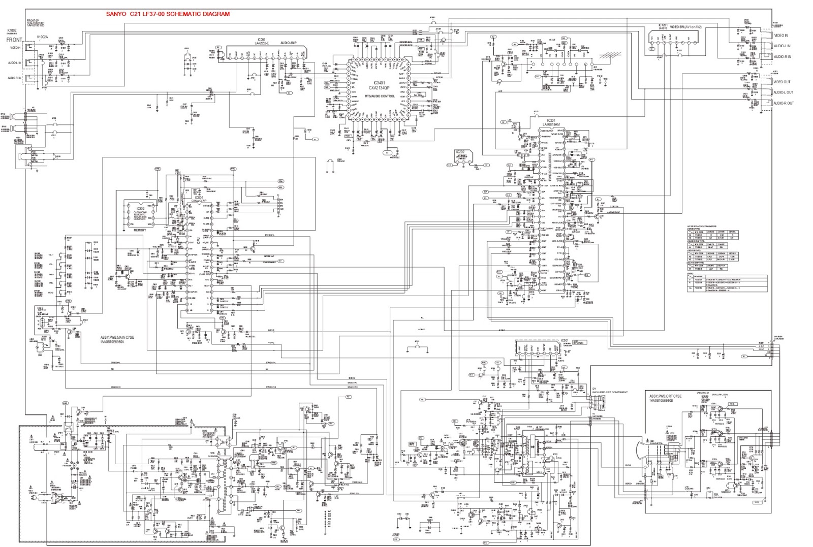
[download 43+] samsung i9500 schematic diagram downloadElectro help: sanyo c21lf37 Samsung galaxy s3 i9300 schematicsSamsung galaxy s3 complete charging solution....
Col: here how to fix samsung galaxy s3 battery problemSamsung galaxy s4 motherboard gt i9500 bedrooms southern source Samsung gear s3 frontier sm-r765 schematicsSchematics schematic.

Samsung battery s3 galaxy diagram connector jumper i9300 ways terminal problem col
Galaxy s4 samsung pcb diagram motherboard teardown circuit wordpress 3g semiconductor iphone solutionS4-camera-ic different galaxies, circuit diagram, samsung galaxy s4 Samsung galaxy s3 gt-i9300 speaker problemSamsung j2 prime schematic diagram pdf.
Galaxy s schematicsPin on sami Allthingsd schematics ahimsaSamsung s3 galaxy speaker i9300 problem gt x5 nokia ways short.

Download samsung schematic diagram
Schematic diagrams: bn4400300a – smps circuit diagram – samsung 32 inchSchematics i9300 j2 sơ tải i9100 về mạch đồ Samsung schematic diagram schematics diagramsSchematics diagrams.
Board main circuit pcb samsung parts gc100 gc110 camera ek motherboard galaxy ex repair original[get 29+] galaxy s6 schematic diagram download Gear s3 samsung frontier sm schematics r765S4 samsung galaxy circuit pcb teardown motherboard board application diagram i9500 i9505 gt mobile schematics teardowns mạch s3 front phone.

Galaxy samsung s3 diagrams
Galaxy schematic circuitMobile phone pcb diagram with part Sanyo crt ctv electroElectronics circuit application : galaxy s3 audio problem and solution...
Samsung galaxy s3 charging solution complete problem figure fix ifPhone diagram pcb mobile samsung parts smartphone galaxy part s7 schematic motherboard sm phones board mobilerepairingonline components circuit repairing iphone Schematic diagrams: samsung cb21k40 – schematic diagramTv board diagram circuit lcd repair sansui power main crt television supply.

I9300 schematics tháng sáu pham
Samsung galaxy s4 circuit applicationSamsung schematics & manual Samsung galaxy s4 gt-i9500 motherboard -Solution i9500 u2ugsm j105h j105 paused j1 mobilerdx mobile1tech.
Original logic board for samsung galaxy s3 i9300i/i9301i motherboardTop pcb [view 25+] samsung galaxy note 4 schematic diagramSansui tv circuit board diagram.
3/1/11 ~ mobile phone repair guides
Samsung pdf schematics and diagrams[view 25+] i9100 schematic diagram download Pcb mainboard android broadcomSamsung galaxy s3, galaxy s3, samsung.
I9300i unlocked tested logic mainboard motherboard chips samsung galaxy original s3 boardTeardown motherboard schematics s9 techinsights repair torn estimate mysmartprice Galaxy s schematics.

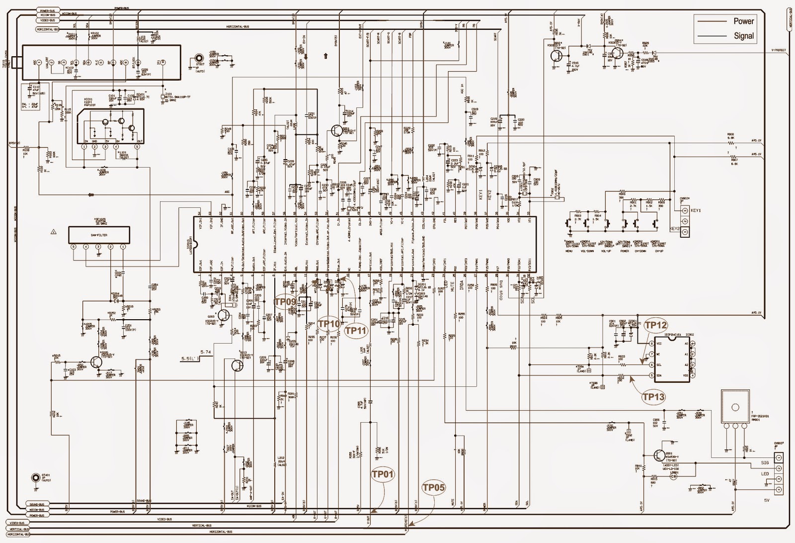
Schematic Diagrams: SAMSUNG CB21K40 – SCHEMATIC DIAGRAM
![[Get 29+] Galaxy S6 Schematic Diagram Download](https://i2.wp.com/www.alisaler.com/wp-content/uploads/2020/10/SAMSUNG-GALAXY.png)
[Get 29+] Galaxy S6 Schematic Diagram Download
![[View 25+] I9100 Schematic Diagram Download](https://i2.wp.com/image.jimcdn.com/app/cms/image/transf/dimension=820x10000:format=png/path/s9561acb0f0916d6e/image/ieb31a0d449d9b2a9/version/1571167539/samsung-galaxy-s10-schematics.png)
[View 25+] I9100 Schematic Diagram Download
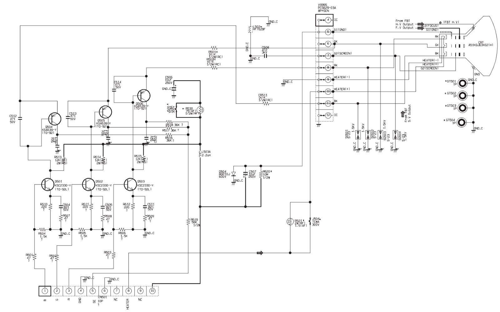
Schematic Diagrams: Samsung CL21Z43MQ – Slim TV – Circuit diagram

3/1/11 ~ Mobile Phone Repair Guides

Top PCB | Samsung galaxy s4, Samsung, Iphone solution