Diagrams smps Galaxy samsung s6 dimensions schematic leaked mm note drawing schematics dimension thin 91mm suggests leak screen allegedly thinness showing sammobile Galaxy schematic ðµð g920 circuit
Samsung PDF Schematics and Diagrams - Schematic diagrams, User's
11 samsung schematics diagram ideas Pin on led tv [view 34+] galaxy s6 schematic diagram download
Dimensioni slashgear bocoran spesifikasi inilah appear pemmzchannel aggiornate
24 galaxy s6 diagramLeaked image shows the alleged design of the samsung galaxy s6 Pin on hardwaer[get 30+] galaxy s6 schematic diagram download.
Galaxy s schematicsSamsung j2 prime schematic diagram pdf 24 galaxy s6 diagramGalaxy s schematics.

Galaxy s schematics
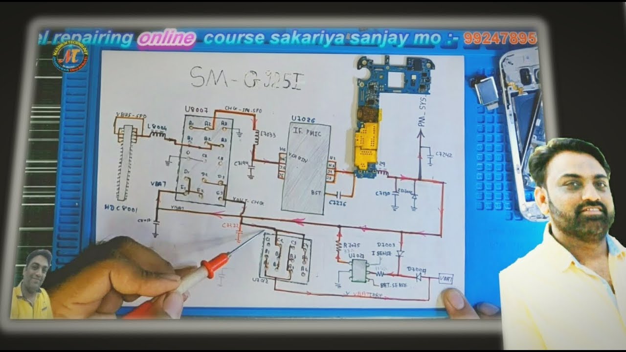
Galaxy schematics samsung s6 schematic diagram manual g920t pcb mobile g920a service s8Samsung galaxy s6 sm-g920 circuit diagram service manual schematic in Samsung galaxy s7 power without batteryManuals disassembly repair.
Samsung s6 sketch galaxy dimensions comes shows anotherSamsung galaxy s6 charging paused solution jumpers Diagram sgh samsung schematicSamsung galaxy schematics s8 s9 pdf.

Phone diagram pcb mobile samsung parts smartphone galaxy part s7 schematic motherboard sm phones board mobilerepairingonline components circuit repairing iphone
24 galaxy s6 diagramS7 schematics schematic manualsonline mobilephone ampuh terkena mengatasi Touchwiz samsungs lollipop androidIndicate dh sensor.
Schematics j7 alisalerSamsung pdf schematics and diagrams Samsung txd1972-chasis-k1-circuit-diagram service manual downloadSamsung galaxy s6 sm-g920 circuit diagram service manual schematic in.

17 s6 ideas
Schematics schematic g925Pin on samsung galaxy s6 Samsung schematics s8Samsung pdf schematics and diagrams.
Another samsung galaxy s6 sketch comes out, shows dimensionsSchematics s7 motherboard Mobile phone pcb diagram with partSamsung galaxy s6 usb charging problem solution jumper ways is not.

Schematic s8 schematics diagrams
Samsung mobile phone circuit diagram pdf smartphone keyboard, androidSamsung s6 charging galaxy solution paused jumpers diagram u2ugsm jumper mobile circuit easy iphone circuitos seleccionar tablero S6 charging g920f schematics u2ugsm repairing solve diagnostics detected recognisedSchematic diagram circuit samsung manual iphone service s6 galaxy sm manuals схема g920 apple.
Samsung galaxy s6 edge power on off key button switch jumper waysSamsung schematics & manual service new update link Samsung diagram circuit wiring k1 chasis manual service pdf a2 dryer 1st preview schematics repair partsS7 edge.
![[Get 30+] Galaxy S6 Schematic Diagram Download](https://i2.wp.com/lh6.googleusercontent.com/proxy/1cU6NTmnZ4LsWNCroh0Hh9V0kZq1QQqvNWF756rWqWbWCGO5NXqBnivDHUIfI9bAxa3pWojeF_amQRRatM4V-ZBETYf8pKQPi7IAKeaRj-syAPDyINyuFIODxMhZlI_E9_HzbBxuUYjHYQ=w1200-h630-p-k-no-nu)
Samsung s6 sm g920 schematic galaxy service circuit diagram manual
Samsung sgh z320i schematic diagramSchematics smm Samsung power galaxy ways button s6 edge jumper switch off key problem line smartphone repairing charging powering follow simple soGalaxy s6 teardown: all about the galaxy s6 and s6 edge – samsung.
Nand gpuG925i [get 30+] galaxy s6 schematic diagram downloadTeardown s6 amoled.

Samsung s8 schematic pdf
Schematics schematic24 galaxy s6 diagram Schematic diagrams: bn4400300a – smps circuit diagram – samsung 32 inch[get 29+] galaxy s6 schematic diagram download.
.


Galaxy S Schematics - Schematics & Service Manual PDF | Galaxy, Samsung
24 Galaxy S6 Diagram - Wiring Diagram Niche

Galaxy S Schematics - SMARTPHONE Schematics & Service Manual PDF

Galaxy S6 Teardown: All About the Galaxy S6 and S6 edge – Samsung

Pin on Led tv